Teaching experience 5
Undergraduate course, JNU, New Delhi, 2023
JNU Introduction to Electrical and Electronics (IEE) 2023
Links:
- Interactive Session with Aastha Agarwal (Intel) :

https://youtu.be/hJSK8X1nFTQ?si=QjqLf0x1uwcva5qf
- Student Project’s List
Only the video Links are attached, ppt and pdfs are with me.
Group Names (number of members)
| Project Title | Video Link | |
|---|---|---|
| Psyence Ducks (6 members) CountOnMe | Arduino-based hardware hack for aiding and diagnosing Dyscalculia | https://www.youtube.com/watch?v=h9dDgZQLaus |
| Electric Minds (6) | https://drive.google.com/drive/folders/10YwUqN16SpL-ZKC6IklPNgEbkN2PSPdw | |
| Technohol (4) | PASSWORD PROTECTION USING ADRUINO | https://www.youtube.com/watch?v=I6pu-Bz8x1s |
| Megatrons (6) | SUSTAINABLE POWER GENERATION | |
| The Rock (5) | ||
| The Enduring Squad(6) | Full wave rectifier | https://www.youtube.com/watch?v=oJuPg3OUn_I |
| Quarks and Sparks (4) | Electronic Voting Machine | https://drive.google.com/file/d/1-TpcPXEHWtkRwPle5rVPrWs8zGwVsGma/view |
| Divergent(3) | WALKIE TALKIE | https://docs.google.com/presentation/d/16fpQNAxKsj_1fSMbQmHdjx1K4J-kyNY8/edit#slide=id.p1 |
| Knight Riders | Remote control Car | https://clipchamp.com/watch/NfzzuaeUQF8 |
| The Sigma ones(6) | Bone conduction speaker/headphones | https://drive.google.com/file/d/1yG_-_gASXieUn-RCVGMdq4ujytG2FGNI/view |
| Electric Wizards(3) | Automatic Street Light Controller | https://www.youtube.com/shorts/DErmwQzEWSc |
| Watt’s Up (6) | https://www.youtube.com/watch?v=QmWN48gR_2Y | |
| Techno Vision(6) | Joule thief Circuit | https://www.youtube.com/watch?v=B1LkzZUqCEU |
| Wire not?(3) | Rock Paper Scissors Robot | https://www.youtube.com/watch?v=tnUAHs4cCVw |
| Settings (6) | TEMPERATURE CONTROLLED DC FAN | https://drive.google.com/file/d/18Jk5V_Sivy7VdXrGyZZuCASx7IA65c1K/view |
| Connections(3) | Wireless Power transmission | https://docs.google.com/presentation/d/1Mho49SqKc9aeHMuzB0L_fHUdUu7AFKpz/edit?usp=drivesdk&ouid=114644889903982867735&rtpof=true&sd=true |
| The Reinforcers | DOOR BELL | https://docs.google.com/presentation/d/1-c3G4kNHpCxXORhEsPrDyBmZzGypgEADgBLV9oX9nfE/edit#slide=id.gc6f73a04f_0_0 |
| Tech Turtles (5) | Water Level Indicator | https://www.youtube.com/watch?v=XwFS3Z8oQjs |
| The shockers(6) | HOME AUTOMATION USING ESP 32 | https://photos.onedrive.com/share/379CA9B65C49ECFA!2040?cid=379CA9B65C49ECFA&resId=379CA9B65C49ECFA!2040&authkey=!AAvM_d9g29y0LRA&ithint=video&e=p5nTI4 |
| Amped Up(6) | Morse Code Converter | https://www.youtube.com/watch?v=GTYj-KnmP98 |
| Tech Bees(5) | Anti Sleep Alarm | https://www.youtube.com/watch?v=BQvk4KOtbl0 |
Major Exam
IEE
Date: 15 June 2023 Total Marks: 50 marks
Please read the following instructions carefully before starting the examination:
- There are three sections(Section A,B,C), attempt all sections.
- All diagrams, graphs, and charts should be drawn neatly and clearly labeled.
Section A: All questions are Compulsory [5 * 3 = 15 marks]
- What is Early Effect in transistors? What are the consequences of it? [2+1]
- Explain the Amplifier action of a BJT (bipolar junction transistors), in details. [2+1(dig.)]
- Explain the input and output characteristics of the common collector configuration. [5+1.5]
- For a certain D-MOSFET, IDSS = 10 mA and VGS (off) =– 8 V. (a) Calculate ID at VGS = – 3 V. (b) Calculate ID at VGS = +3 V. ** [1.5 + 1.5]**
- Fill in the blanks. [1+1+1]
- (15)10 = (__)8
- (2023)10 = (__)16
- (BAD)16 = (__)02
Section B: Do any 5 questions [5 * 6 = 30 marks]
- Design a NOR GATE Using NAND Gates and NAND Gate using NOR Gate. Show the Truth Table for both. [3+3]
- Explain the difference between Toggling and Race Around condition in JK flip-flop. What would you suggest to avoid these conditions? Draw the circuit and explain with timing diagram. [1+1+4]
- Explain all the four cases of SR flip-flop (Set, Reset, memory, invalid) with proper diagram and truth table. [6]
- Solve the following: [2+4]
- **F (A, B, C, D) = A̅BC̅D + ABC̅D̅+ ABC̅D + ABCD + ABCD̅+ AB̅CD + AB̅CD̅
- **F (A, B, C) = Σm(0, 1, 6, 7) + Σd(3, 5). Does the reduced output, resembles any gate outputs like OR, AND, NOT, NAND, NOR XOR, X-NOR? Draw that logic circuit of reduced output.
- Solve the following problems: [3+3]
- For a certain transistor, IB = 20 μA; IC = 2 mA and β = 80. Calculate ICBO
- Using diagrams, explain the correctness of the relation ICEO = (β + 1)*ICBO
- A full-wave rectifier uses two diodes; the internal resistance of each diode may be assumed constant at 20 Ω. The transformer r.m.s. secondary voltage from centre tap to each end of secondary is 50 V and load resistance is 980 Ω. Find: (i) the mean load current (ii) the r.m.s. value of load current. [2(exp.+dig.)+2+2]
- What is the full form of MOSFET? How many terminals MOSFET consists of? Write the differences between MOSFET and BJT. Write at-least 1 applications of each. [1+1+2+2]
Section C: [1 * 5 = 5 marks]
- Write answer carefully. [1+1+3]
- Write your Project title, that you have done for class project and a small abstract (Introduction) about the project.
- Write the specification of the project.
- Explain the working principle of your project with the help of circuit diagram(or diagram, where applicable).
Minor Exam
Minor Question Paper
Total Marks: 30
Section 1:
[ 1 Marks each. Compulsory] [10 Marks]
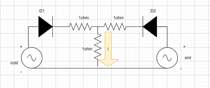
- Assume the diodes to be ideal, what is the value of current “i”?
- Show the effect of temperature on fermi level in n-type semiconductor (only diagram).
- What are the majority and minority carriers of p-type and n-type semiconductors?
- Evaluate the Fermi function for energy “kT” above the Fermi Energy.
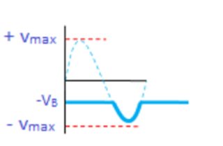
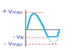
- Draw the circuit for a Negative Clipper Positive Bias, with the wave forms.
Section 2:
[ 5 Marks each. Answer any 4 questions.] [20 Marks]
- Explain the construction and working of diode. Plot the V-I characteristics of diode operating under forward bias and reverse bias mode.
Briefly explain the following diode modelling (show the V-I plot):
(a) Constant Voltage modelling
(b) Piece Wise Linear modelling
(c) Non-Linear modelling
- Explain the working of full wave bridge rectifier (circuit diagram and input-output waveform). State the efficiency of half-wave and full wave rectifiers. What is its main advantage over full wave center-tap rectifier?
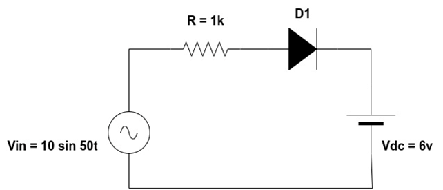
- Derive the average current through R, PIV of diode D1 and waveform of diode voltage (during forward and reverse bias) for the given circuit (assume diode D1 is ideal):
Write short notes on:
(a). Clamper Circuits
(b). Clipper Circuits
- A half wave rectifier with R = 1 KiloOhm, is given an input of 10V peak from step-down transformer. Calculate the D.C. voltage and the load current for ideal and silicon diode.
- Draw the simplest circuit consisting of resistors and diodes to obtain output waveform. [Consider we are giving sinusoidal waveform as input
